Instrukcja obsługi Microchip HV7350DB1
Microchip Niesklasyfikowane HV7350DB1
Przeczytaj poniżej 📖 instrukcję obsługi w języku polskim dla Microchip HV7350DB1 (10 stron) w kategorii Niesklasyfikowane. Ta instrukcja była pomocna dla 15 osób i została oceniona przez 8 użytkowników na średnio 4.0 gwiazdek
Strona 1/10
Supertex inc.
Supertex inc.
www.supertex.com
HV7350DB1
Doc.# DSDB-HV7350DB1
A070214
General Description
The HV7350 is a monolithic eight channel, high-speed, high
voltage, ultrasound transmitter RTZ pulser. This integrated,
high performance circuit is in a single, 8x8x0.9 mm, 56-lead
QFN package.
The HV7350 can deliver a guaranteed ±1.0A source and
sink current to a capacitive transducer with +/-60V peak to
peak voltage. It is designed for portable medical ultrasound
imaging and ultrasound NDT applications. It can also be used
as a high voltage driver for other piezoelectric or capacitive
MEMS transducers, or for test systems as a signal source or
pulse signal generators.
The HV7350’s circuitry consists of controller logic circuits,
level translators, gate driving buffers and a high current and
high voltage MOSFET output stage. The output stages of
each channel are designed to provide peak output currents
typically over ±1.0A for pulsing, with up to ±60V swings in
RTZ mode. The upper limit frequency of the pulser waveform
is depending on the load capacitance.
This demoboard datasheet describes how to use the
HV7350DB1 to generate the basic high voltage pulse
waveform as an ultrasound transmitting pulser.
The HV7350 circuit uses DC coupling from a 3.3V logic
input to output Tx1~8 internally, therefore the chip needs
three sets of voltage supply rails: V
LL
+3.3V, V
DD
+5.0V and
V
PP
/V
NN
±10 to ±60V. The V
PP
and V
NN
rail voltages can be
changed rather quickly, compared to the capacitor gate-
coupled driving pulsers. This direct coupling topology of the
gate drivers not only saves two high voltage capacitors per
channel, but also makes the PCB layout easier.
The HV7350DB1 output waveforms can be displayed using
an oscilloscope by connecting the scope probe directly to
the test points TX1~8 and GND. The soldering jumper can
select whether or not to connect the on-board dummy-load,
a 330pF capacitor paralleling with a 2.5kΩ resistor. The test
points can be used to connect the user’s transducer to easily
evaluate the pulser.
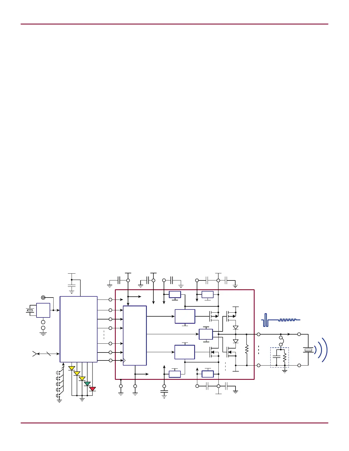
Block Diagram
Eight Channel ±60V, ±1.0A,
Ultrasound Pulser Demoboard
CPFVDD
+3.3V
RGND
HV
OUT
1
VPP
+10 to +60V
-10 to -60V
P-Driver
N-Driver
1 of 8 Channels
VLL
Logic
&
Level
Translator
-5V
RGND
RGND
DMP
1.0µF
VPF
VNF
Rb
LRP
+5.0V
CPOS
GND
GND
SUB
+4.0V
V
REF
REN
OEN
PIN1
NIN1
PIN8
NIN8
CLK
DAP
LRP
GND
LRN
GND
VNF
VPF
LRN
GND
GNDCNEGCNFVNN
+5.0V
-5.0V
1.0µF
1.0µF
0.1µF1.0µF1.0µF
TX1
+3.3V
1.0µF1.0µF
RGND
TX1
Waveform
Generator
CPLD
OSC
JTAG
EXCLK
EN
CLK
IN
WAVE
FREQ
PHAS
OEN
REN
RTZ
PHAS
PWR
OEN
REN
40MHz
6
+3.3V
C4
330pF
R2
R3
2.5k
Dummy
Load
Specyfikacje produktu
| Marka: | Microchip |
| Kategoria: | Niesklasyfikowane |
| Model: | HV7350DB1 |
Potrzebujesz pomocy?
Jeśli potrzebujesz pomocy z Microchip HV7350DB1, zadaj pytanie poniżej, a inni użytkownicy Ci odpowiedzą
Instrukcje Niesklasyfikowane Microchip

15 Stycznia 2025
15 Stycznia 2025
15 Stycznia 2025
15 Stycznia 2025
15 Stycznia 2025
15 Stycznia 2025
15 Stycznia 2025
15 Stycznia 2025
15 Stycznia 2025
15 Stycznia 2025
Instrukcje Niesklasyfikowane
Najnowsze instrukcje dla Niesklasyfikowane
29 Stycznia 2025
29 Stycznia 2025
29 Stycznia 2025
29 Stycznia 2025
29 Stycznia 2025
29 Stycznia 2025
29 Stycznia 2025
29 Stycznia 2025
29 Stycznia 2025
29 Stycznia 2025