Instrukcja obsługi Steren SN74LS47N
Steren Niesklasyfikowane SN74LS47N
Przeczytaj poniżej 📖 instrukcję obsługi w języku polskim dla Steren SN74LS47N (8 stron) w kategorii Niesklasyfikowane. Ta instrukcja była pomocna dla 13 osób i została oceniona przez 3 użytkowników na średnio 4.7 gwiazdek
Strona 1/8
Semiconductor Components Industries, LLC, 1999
December, 1999 – Rev. 6
1Publication Order Number:
SN74LS47/D
SN74LS47
BCDto7-Segment
Decoder/Driver
The SN74LS47 are Low Power Schottky BCD to 7-Segment
Decoder/Drivers consisting of NAND gates, input buffers and seven
AND-OR-INVERT gates. They offer active LOW, high sink current
outputs for driving indicators directly. Seven NAND gates and one
driver are connected in pairs to make BCD data and its complement
available to the seven decoding AND-OR-INVERT gates. The
remaining NAND gate and three input buffers provide lamp test,
blanking input/ripple-blanking output and ripple-blanking input.
The circuits accept 4-bit binary-coded-decimal (BCD) and,
depending on the state of the auxiliary inputs, decodes this data to
drive a 7-segment display indicator. The relative positive-logic output
levels, as well as conditions required at the auxiliary inputs, are shown
in the truth tables. Output configurations of the SN74LS47 are
designed to withstand the relatively high voltages required for
7-segment indicators.
These outputs will withstand 15 V with a maximum reverse current
of 250µA. Indicator segments requiring up to 24 mA of current may
be driven directly from the SN74LS47 high performance output
transistors. Display patterns for BCD input counts above nine are
unique symbols to authenticate input conditions.
The SN74LS47 incorporates automatic leading and/or trailing-edge
zero-blanking control (RBI and RBO). Lamp test (LT) may be
performed at any time which the BI/RBO node is a HIGH level. This
device also contains an overriding blanking input (BI) which can be
used to control the lamp intensity by varying the frequency and duty
cycle of the BI input signal or to inhibit the outputs.
•Lamp Intensity Modulation Capability (BI/RBO)
•Open Collector Outputs
•Lamp Test Provision
•Leading/Trailing Zero Suppression
•Input Clamp Diodes Limit High-Speed Termination Effects
GUARANTEED OPERATING RANGES
SymbolParameterMinTypMaxUnit
V
CC
Supply Voltage4.755.05.25V
T
A
Operating Ambient
Temperature Range
02570°C
I
OH
Output Current – High
BI/RBO
–50
m
A
I
OL
Output Current – Low
BI/RBO
BI/RBO
3.2mA
V
O(off)
Off–State Output Voltage
a to g
15V
I
O(on)
On–State Output Current
a to g
24mA
LOW
POWER
SCHOTTKY
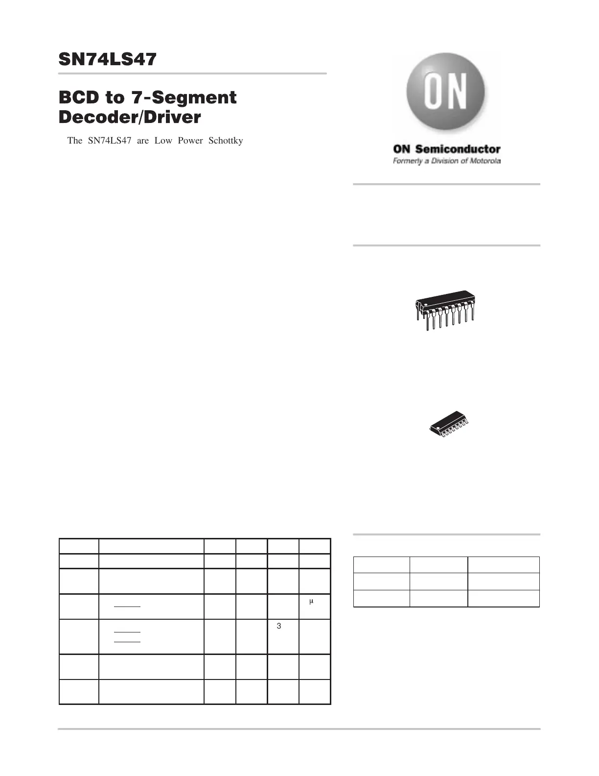
SOIC
D SUFFIX
CASE 751B
http://onsemi.com
PLASTIC
N SUFFIX
CASE 648
16
1
16
1
DevicePackageShipping
ORDERING INFORMATION
SN74LS47N16 Pin DIP2000 Units/Box
SN74LS47D16 Pin
2500/Tape & Reel
Specyfikacje produktu
| Marka: | Steren |
| Kategoria: | Niesklasyfikowane |
| Model: | SN74LS47N |
Potrzebujesz pomocy?
Jeśli potrzebujesz pomocy z Steren SN74LS47N, zadaj pytanie poniżej, a inni użytkownicy Ci odpowiedzą
Instrukcje Niesklasyfikowane Steren

24 Września 2024
24 Września 2024
24 Września 2024
24 Września 2024
24 Września 2024
24 Września 2024
24 Września 2024
23 Września 2024
23 Września 2024
22 Września 2024
Instrukcje Niesklasyfikowane
Najnowsze instrukcje dla Niesklasyfikowane
29 Stycznia 2025
29 Stycznia 2025
29 Stycznia 2025
29 Stycznia 2025
29 Stycznia 2025
29 Stycznia 2025
29 Stycznia 2025
29 Stycznia 2025
29 Stycznia 2025
29 Stycznia 2025